|
8086 CPU ARCHITECTURE The microprocessors
functions as the CPU in the stored program model of the digital computer. Its
job is to generate all system timing signals and synchronize the transfer of data
between memory, I/O, and itself. It accomplishes this task via the three-bus
system architecture previously discussed. The microprocessor also
has a S/W function. It must recognize, decode, and
execute program instructions fetched from the memory unit. This requires an
Arithmetic-Logic Unit (ALU) within the CPU to perform arithmetic and logical
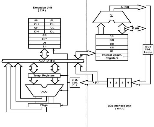
(AND, OR, NOT, compare, etc) functions. The 8086 CPU is organized
as two separate processors, called the Bus Interface Unit (BIU) and the
Execution Unit (EU). The BIU provides H/W functions, including generation of
the memory and I/O addresses for the transfer of data between the outside world
-outside the CPU, that is- and the EU. The EU receives program
instruction codes and data from the BIU, executes these instructions, and store
the results in the general registers. By passing the data back to the BIU, data
can also be stored in a memory location or written to an output device. Note
that the EU has no connection to the system buses. It receives and outputs all
its data thru the BIU.
The only difference
between an 8088 microprocessor and an 8086 microprocessor is the BIU. In the
8088, the BIU data bus path is 8 bits wide versus the 8086's 16-bit data bus.
Another difference is that the 8088 instruction queue is four bytes long
instead of six. The important point to
note, however, is that because the EU is the same for each processor, the
programming instructions are exactly the same for each. Programs written for
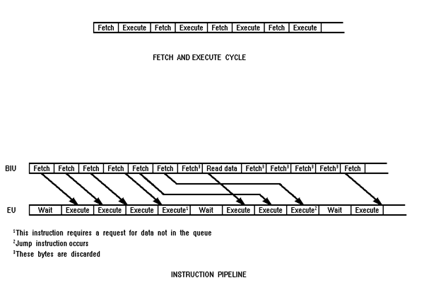
the 8086 can be run on the 8088 without any changes. FETCH AND EXECUTE Although the 8086/88
still functions as a stored program computer, organization of the CPU into a
separate BIU and EU allows the fetch and execute cycles to overlap. To see
this, consider what happens when the 8086 or 8088 is first started. 1. The BIU outputs the
contents of the instruction pointer register (IP) onto the address bus, causing
the selected byte or word to be read into the BIU.
The BIU is programmed to
fetch a new instruction whenever the queue has room for one (with the 8088) or
two (with the 8086) additional bytes. The advantage of this pipelined
architecture is that the EU can execute instructions almost continually instead
of having to wait for the BIU to fetch a new instruction. There are three
conditions that will cause the EU to enter a "wait" mode. The first
occurs when an instruction requires access to a memory location not in the
queue. The BIU must suspend fetching instructions and output the address of
this memory location. After waiting for the memory access, the EU can resume
executing instruction codes from the queue (and the BIU can resume filling the
queue). The second condition
occurs when the instruction to be executed is a "jump" instruction.
In this case control is to be transferred to a new (nonsequential)
address. The queue, however, assumes that instructions will always be executed
in sequence and thus will be holding the "wrong" instruction codes.
The EU must wait while the instruction at the jump address is fetched. Note
that any bytes presently in the queue must be discarded (they are overwritten).
One other condition can
cause the BIU to suspend fetching instructions. This occurs during execution of
instructions that are slow to execute. For example, the instruction AAM (ASCII
Adjust for Multiplication) requires 83 clock cycles to complete. At four cycles
per instruction fetch, the queue will be completely filled during the execution
of this single instruction. The BIU will thus have to wait for the EU to pull
over one or two bytes from the queue before resuming the fetch cycle. A subtle advantage to the
pipelined architecture should be mentioned. Because the next several
instructions are usually in the queue, the BIU can access memory at a somewhat
"leisurely" pace. This means that slow-mem
parts can be used without affecting overall system performance. PROGRAMING MODEL As a programmer of the
8086 or 8088 you must become familiar with the various registers in the EU and
BIU.
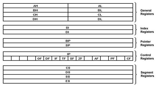
The data group consists
of the accumulator and the BX, CX, and DX registers. Note that each can be
accessed as a byte or a word. Thus BX refers to the 16-bit base register but BH
refers only to the higher 8 bits of this register. The data registers are
normally used for storing temporary results that will be acted on by subsequent
instructions. The pointer and index
group are all 16-bit registers (you cannot access the low or high bytes alone).
These registers are used as memory pointers. Sometimes a pointer reg will be interpreted as pointing to a memory byte and at
other times a memory word. As you will see, the 8086/88 always stores words
with the high-order byte in the high-order word address. Register IP could be
considered in the previous group, but this register has only one function -to
point to the next instruction to be fetched to the BIU. Register IP is
physically part of the BIU and not under direct control of the programmer as
are the other pointer registers. Six of the flags are
status indicators, reflecting properties of the result of the last arithmetic
or logical instructions. The 8086/88 has several instructions that can be used
to transfer program control to a new memory location based on the state of the
flags. Three of the flags can be
set or reset directly by the programmer and are used to control the operation
of the processor. These are TF, IF, and DF. The final group of
registers is called the segment group. These registers are used by the BIU to
determine the memory address output by the CPU when it is reading or writing
from the memory unit. To fully understand these registers, we must first study
the way the 8086/88 divides its memory into segments. SEGMENTED MEMORY Even though the 8086 is
considered a 16-bit processor, (it has a 16-bit data bus width) its memory is
still thought of in bytes. At first this might seem a disadvantage: Why saddle a 16-bit
microprocessor with an 8-bit memory? Actually, there are a
couple of good reasons. First, it allows the processor to work on bytes as well
as words. This is especially important with I/O devices such as printers,
terminals, and modems, all of which are designed to transfer ASCII-encoded (7-
or 8-bit) data. Second, many of the
8086's (and 8088's) operation codes are single bytes. Other instructions may
require anywhere from two to seven bytes. By being able to access individual
bytes, these odd-length instructions can be handled. We have already seen that
the 8086/88 has a 20-bit address bus, allowing it to output 210, or
1'048.576, different memory addresses. As you can see, 524.288 words can also
be visualized. As mentioned, the 8086
reads 16 bits from memory by simultaneously reading an odd-addressed byte and
an even-addressed byte. For this reason the 8086 organizes its memory into an
even-addressed bank and an odd-addressed bank. With regard to this, you
might wonder if all words must begin at an even address. Well, the answer is
yes. However, there is a penalty to be paid. The CPU must perform two memory
read cycles: one to fetch the low-order byte and a second to fetch the
high-order byte. This slows down the processor but is transparent to the
programmer. The last few paragraphs
apply only to the 8086. The 8088 with its 8-bit data bus interfaces to the 1 MB
of memory as a single bank. When it is necessary to access a word (whether on
an even- or an odd-addressed boundary) two memory read (or write) cycles are
performed. In effect, the 8088 pays a performance penalty with every word
access. Fortunately for the programmer, except for the slightly slower
performance of the 8088, there is no difference between the two processors. MEMORY MAP Still another view of the
8086/88 memory space could be as 16 64K-byte blocks beginning at hex address
000000h and ending at address 0FFFFFh. This division into 64K-byte blocks is an
arbitrary but convenient choice. This is because the most significant hex digit
increments by 1 with each additional block. That is, address 20000h is 65.536
bytes higher in memory than address 10000h. Be sure to note that five hex
digits are required to represent a memory address.
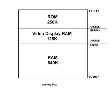
The diagram is called a
memory map. This is because, like a road map, it is a guide showing how the
system memory is allocated. This type of information is vital to the
programmer, who must know exactly where his or her programs can be safely
loaded. Note that some memory
locations are marked reserved and others dedicated. The dedicated locations are
used for processing specific system interrupts and the reset function. Intel
has also reserved several locations for future H/W and S/W products. If you
make use of these memory locations, you risk incompatibility with these future
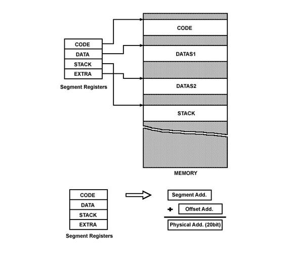
products. SEGMENT REGISTERS Within the 1 MB of memory
space the 8086/88 defines four 64K-byte memory blocks called the code segment,
stack segment, data segment, and extra segment. Each of these blocks of memory
is used differently by the processor. The code segment holds
the program instruction codes. The data segment stores data for the program.
The extra segment is an extra data segment (often used for shared data). The
stack segment is used to store interrupt and subroutine return addresses. You should realize that
the concept of the segmented memory is a unique one. Older-generation
microprocessors such as the 8-bit 8086 or Z-80 could access only one 64K-byte
segment. This mean that the programs instruction, data and subroutine stack all
had to share the same memory. This limited the amount of memory available for
the program itself and led to disaster if the stack should happen to overwrite
the data or program areas. The four segment
registers (CS, DS, ES, and SS) are used to "point" at location 0 (the
base address) of each segment. This is a little "tricky" because the
segment registers are only 16 bits wide, but the memory address is 20 bits
wide. The BIU takes care of this problem by appending four 0's to the low-order
bits of the segment register. In effect, this multiplies the segment register
contents by 16.
The point to note is that
the beginning segment address is not arbitrary -it must begin at an address
divisible by 16. Another way if saying this is that the low-order hex digit
must be 0. Also note that the four
segments need not be defined separately. Indeed, it is allowable for all four
segments to completely overlap (CS = DS = ES = SS). Memory locations not
defined to be within one of the current segments cannot be accessed by the
8086/88 without first redefining one of the segment registers to include that
location. Thus at any given instant a maximum of 256 K (64K * 4) bytes of
memory can be utilized. As we will see, the contents of the segment registers
can only be specified via S/W. As you might imagine, instructions to load these
registers should be among the first given in any 8086/88 program. LOGICAL AND PHYSICAL
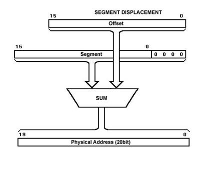
ADDRESS Addresses within a
segment can range from address 00000h to address 0FFFFh. This corresponds to
the 64K-byte length of the segment. An address within a segment is called an
offset or logical address. A logical address gives the displacement from the
address base of the segment to the desired location within it, as opposed to
its "real" address, which maps directly anywhere into the 1 MB memory
space. This "real" address is called the physical address. What is the difference between
the physical and the logical address? The physical address is
20 bits long and corresponds to the actual binary code output by the BIU on the
address bus lines. The logical address is an offset from location 0 of a given
segment.
When two segments overlap
it is certainly possible for two different logical addresses to map to the same
physical address. This can have disastrous results when the data begins to
overwrite the subroutine stack area, or vice versa. For this reason you must be
very careful when segments are allowed to overlap. You should also be
careful when writing addresses on paper to do so clearly. To specify the
logical address XXXX in the stack segment, use the convention SS:XXXX, which is equal to [SS] * 16 + XXXX. ADVANTAGES OF
SEGMENTED MEMORY Segmented memory can seem
confusing at first. What you must remember is that the program op-codes will be
fetched from the code segment, while program data variables will be stored in
the data and extra segments. Stack operations use registers BP or SP and the
stack segment. As we begin writing programs the consequences of these
definitions will become clearer. An immediate advantage of
having separate data and code segments is that one program can work on several
different sets of data. This is done by reloading register DS to point to the
new data. Perhaps the greatest advantage of segmented memory is that programs
that reference logical addresses only can be loaded and run anywhere in memory.
This is because the logical addresses always range from 00000h to 0FFFFh,
independent of the code segment base. Such programs are said to be relocatable, meaning that they will run at any location in
memory. The requirements for writing relocatable
programs are that no references be made to physical addresses, and no changes
to the segment registers are allowed.
REFERENCE
Books The 80x86 IBM PC and Compatible Computers (Vol 1 and Vol 2) Microcomputer Systems: The 8086/8088 Family
Online
Materials Intel Developers website �
http://developer.intel.com AIX-86 (8086) Datasheet |